

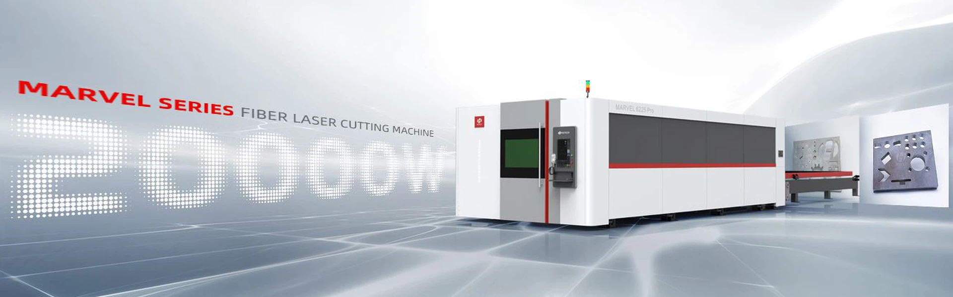


Wafer Laser Cutting Machine
Product advantages:
High quality
There is no damage on the surface, no cutting seam, and the edge collapse is very small (≤ 2 μ m) , the edge is small (< 3 μ m)
High efficiency
Multi focus modification mode can be adopted to multiply the cutting efficiency
Good stability
The laser has high average power stability (≤± 3% over 24 hours) and high beam quality (M ² < 1.5)

|
Item |
Main parametetrs |
|
|
Laser |
Center wavelength |
Custom infrared wavelength |
|
Cutting head |
Self-developed collimating head | |
|
Performance |
Effective working stroke |
300x400mm(optional) |
|
Repetitive positioning accuracy |
±1μm |
|
|
Visual positioning |
Automatic visual positioning |
|
|
Processing method |
Layer by layer upgrading, single point / multi-point processing | |
|
Others |
Wafer size |
8 inch (12inch is compatible ) |
|
Processing process |
Laser modified cutting - film spreading | |
|
Processing object |
MEMS chip, silicon-based biochip, silicon wheat chip, CMOS chip, etc | |
Silicon Wafer Dicing:
Precision cutting of 200mm/300mm silicon wafers for integrated circuits (ICs)
Minimizes chipping and defects during dicing process
MEMS Device Fabrication:
Ultra-precision laser scribing for microelectromechanical systems (MEMS)
Suitable for thin-film sensors and actuators
IC Packaging:
Accurate die separation for advanced packaging techniques (Fan-out, 3D stacking)
Solar Cell Production:
Compatible with silicon and compound semiconductor materials
Unique Selling Points:
- Non-Contact Cutting: Avoids mechanical stress and contamination
- Real-Time Monitoring: AI-powered system detects defects during processing
- Energy Efficiency: Low power consumption compared to traditional cutting methods
- Customizable Parameters: Adjustable laser power and pulse frequency


Product FAQs:
Q1: What is the maximum wafer size this laser cutter can handle for semiconductor applications?
A: Our equipment supports wafers up to 300mm x 300mm, making it ideal for large-scale IC and MEMS production.
Q2: How does the laser cutting minimize thermal damage to silicon wafers?
A: We use a 1064nm fiber laser with precise pulse control and real-time temperature monitoring to ensure a heat-affected zone (HAZ) of less than 1μm, protecting wafer integrity.
Q3: Is the equipment compatible with cleanroom environments in semiconductor fabs?
A: Yes! Our machines meet ISO Class 1000 cleanroom standards and feature contamination-resistant designs for IC packaging and MEMS fabrication.
Q4: Can the wafer laser cutting system process non-silicon materials like GaAs or quartz?
A: Absolutely. The system is compatible with silicon, quartz, glass, and GaAs, supporting diverse applications in photonics and compound semiconductor manufacturing.
Q5:What is the typical throughput for high-volume wafer dicing?
A: With our automated alignment system, the machine achieves up to 500 wafers/hour (varies by pattern complexity), ensuring efficient production for semiconductor fabs.
Hot Tags: wafer laser cutting machine, manufacturers, suppliers, price, for sale
Send Inquiry


